Jump directly to main navigation Jump directly to content Jump to sub navigation

Smart laser sensors measure extremely fine details in electronics production

ME468_Header.JPG

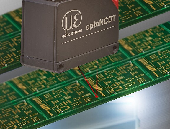
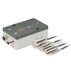
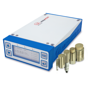
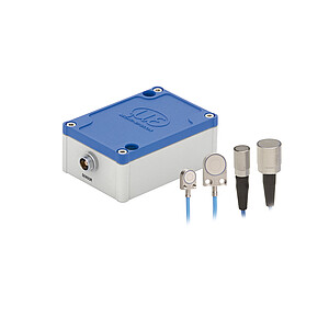
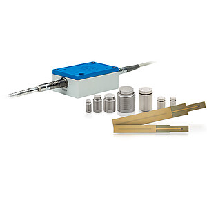
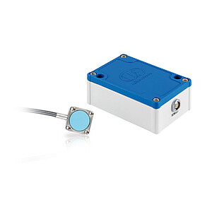
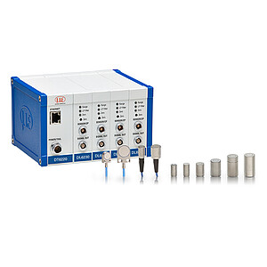
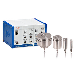
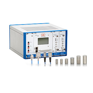
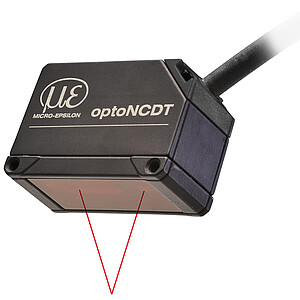
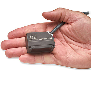
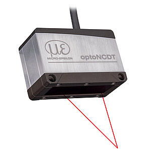
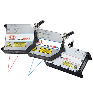
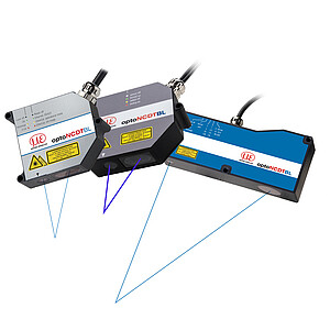
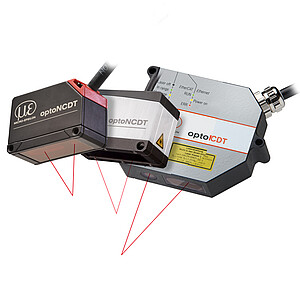
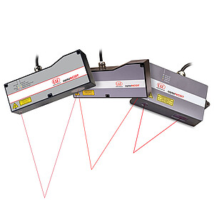
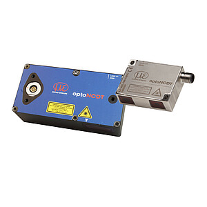
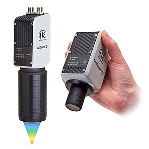
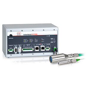
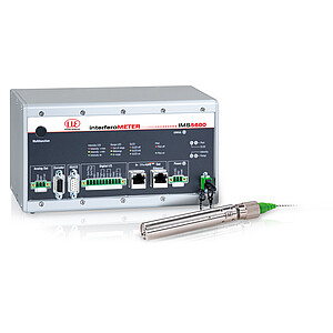
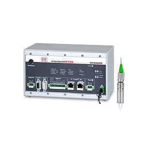
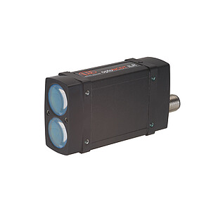
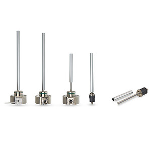
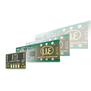
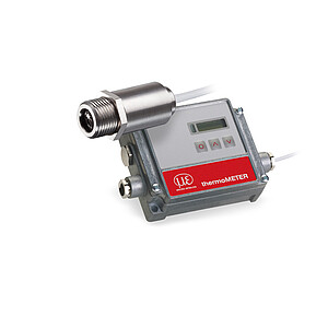
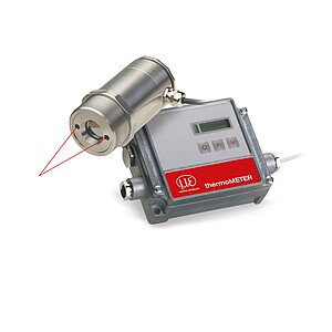
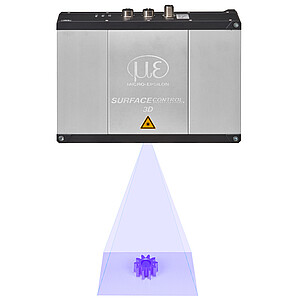
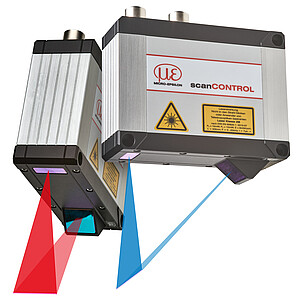
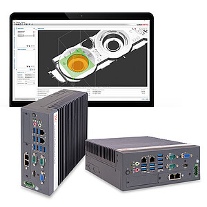
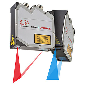
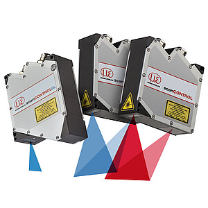
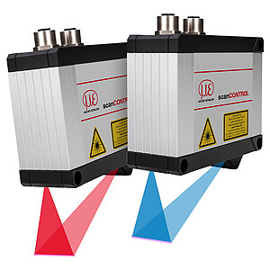
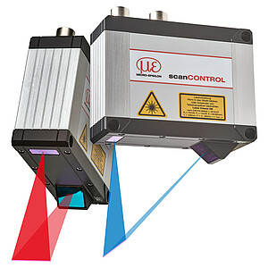
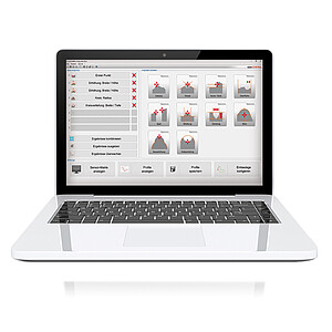
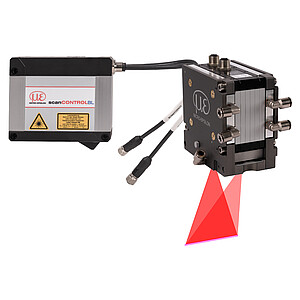
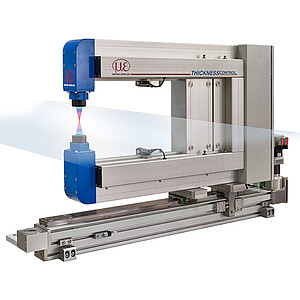
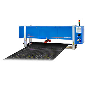
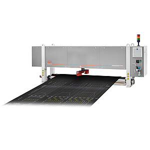
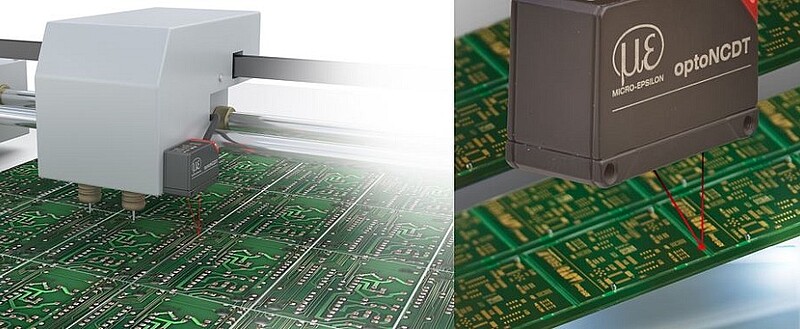
In PCB manufacturing, extremely high precision and high production speeds are required. Smart displacement sensors can be used in pick-and-place machines, where they perform reliable quality inspection at micrometer accuracies. In PCB production, the sensors can also inspect the position of integrated components and measure the scribe lines of PCB panels, says Glenn Wedgbrow, Business Development Manager at Micro-Epsilon UK.

Whether a smartphone, medical device or machine tool – almost every electrical device has a printed circuit board (PCB). However, these devices are getting smaller, more efficient and faster, whereas the development cycles are becoming increasingly shorter. This also means that the boards must become significantly more powerful by using highly integrated components. Miniaturisation of switches and individual components, as well as ever increasing packing density, are essential elements to fulfill the required performance. In order to ensure that current – in the form of electrical energy signals or as information signals – easily flows through the components, exact positioning of electronic components is crucial. In PCB manufacturing, these must not only be in the right place but also on the right level in order to connect them properly. For smooth functioning, the components must not be tilted.

High measuring requirements

Sensors that inspect the position of highly-integrated components during production must overcome a series of challenges. Primarily, these include high speeds due to the highly dynamic production process, a small focus diameter because of extremely small components, and high spatial resolution due to minimal displacement changes that must be detected. The optoNCDT 1420 series of smart laser triangulation sensors from Micro-Epsilon is designed for high-tech applications. These laser sensors measure on a non-contact basis and do not affect the PCB or its highly-sensitive components. The non-contact measuring procedure enables the laser sensors to acquire and process the measurement values very quickly. The most important characteristics of laser triangulation sensors are their high performance, extremely compact design and reliable signal adjustment on changing surfaces, which ensures high precision results.

Quality control in electronics

In quality control of PCB production, the sensors are placed in such a way that they measure the PCB from above. A traversing system guides them over the PCBs and its highly-integrated components. With a measuring rate up to 8 kHz, the sensors can detect dynamic processes directly in the production line. The compactness of the sensor (46 mm x 30 mm) and its integrated controller enable the sensor to be integrated in small installation spaces. The smallest possible diameter of the light spot is just 45 µm x 40 µm, which enables high precision measurements on fine IC pins as the light spot can be sharply focussed onto them.

Another critical factor for reliable measurements on PCBs is to use a measuring procedure that can measure different materials, from plastics to metals, which is why the laser triangulation principle is the correct choice. Laser triangulation sensors from Micro-Epsilon provide the innovative Auto Target Compensation (short: ATC) feature that enables the sensors to measure on permanently changing surfaces, from matt black to shiny and reflective targets, as well as from bright to dark. ATC ensures that the exposure time adapts to the conditions presented by the respective target object. To determine the measurement values, the laser sensor projects a red laser point at a wavelength of 670 nm onto the target. The laser light is back-scattered in a certain reflection angle to hit the optical system of a CMOS line. With quickly changing objects from bright to dark, only a little light would reach the receiving matrix without using the ATC feature. In contrast, the intensity would be too high when quickly changing from dark surfaces to shiny objects. In both cases, the result would be inaccurate or even useless. Therefore, the Micro-Epsilon sensor regulates the exposure time via ATC, as well as the intensity of the light emitted during the measurement task in such a way that the reflection on the CMOS line is in the ‘perfect’ range. The sensor then calculates the distance values to micron-accuracy via the three-point relationship between the laser diode, the measuring position on the object and the depiction on the CCD line. The values determined can be fed in as an analogue or digital output signal to the plant or machine control system.

Measuring scribe lines

Another application in PCB manufacture is the scribing of pre-determined breaking points into the panels for de-panelling. A PCB consists of several panels or smaller PCBs that go through production as one large PCB. This kind of bundling is necessary for production reasons as it makes boards easier to assemble. The scribe lines are normally produced by two opposing saw blades that cut a V-groove into the board, which allows small PCBs to be easily and cleanly de-panelled (i.e. separated from one another) by the end of the production processes. The scribe lines are around 400 µm wide.

The scribe lines of PCB panels must be measured precisely. Here, the optoNCDT 1420 laser sensor is also used due its unique combination of speed and precision combined with an extremely compact design. During production, the sensor detects whether the keyway is accurately milled into the panels. If the scribe line is too thin, the panels will break during the production process, which consumes resources and may cause damage to the machines. If the grooves are not milled deeply enough, the panels would fray during de-panelling and break irregularly, which means that they would not fulfil the quality requirements resulting in waste.

Conclusion

Using modern sensors such as the optoNCDT 1420 laser triangulation sensor from Micro-Epsilon helps to improve quality while reducing waste and saving money. The laser sensor reliably measures displacement, distance and position with repeatability from 0.5 µm. Its extremely small measurement spot accurately detects even the smallest of PCB components such as IC pins. With up to 8,000 measurement values per second, the sensor is designed for highly dynamic processes such as those found in the electronics industry and additive manufacturing. A compact design with integrated controller simplifies integration in machines and systems even where installation space is tight. Intelligent surface control balances the fluctuating intensity of the light reflected during the measurement process when colour or brightness change rapidly. Particularly with PCBs – where matt and shiny, as well as bright and dark objects are side by side – this is a major advantage in order to achieve stable and micrometer-accurate results. The intuitive web interface allows the user to configure the sensor and offers predefined presets for different measurement tasks. Furthermore, up to eight user-specific settings can be stored and exported. The video signal display, signal peak selection and a freely adjustable signal averaging, enable the measurement task to be optimised. The region of interest (ROI) function allows, for example, interference signals to be filtered out. Fast commissioning is also possible.

For more information, please visit www.micro-epsilon.co.uk or call the Micro-Epsilon sales department on +44 (0)151 355 6070 or email info@~@micro-epsilon.co.uk

Further Information